1D Photonic Crystal
The most simple photonic crystal structure is a one dimensional system consisting of alternating layers with different permittivities, i.e. a multilayer film. In this tutorial example a band diagram for a 1D photonic crystal is computed. This is achieved by determining the resonance mode frequencies of the one dimensional structure and scanning the Bloch vector to produce the following band structure.
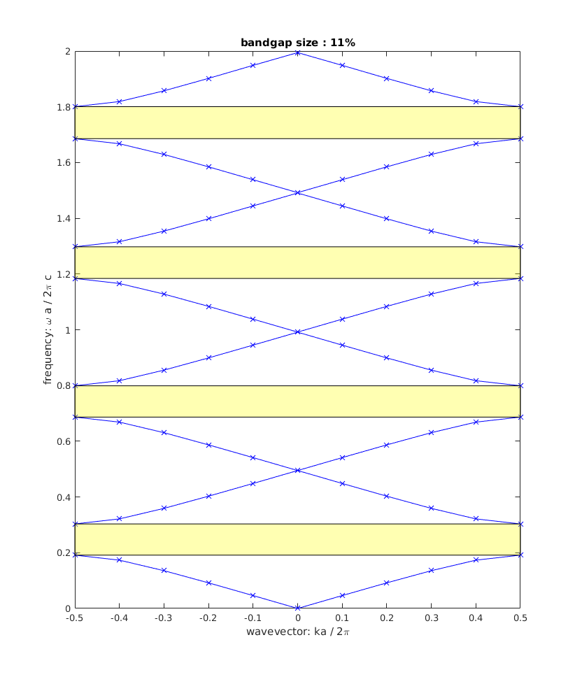
Photonic band structure in normalized frequency and wave vector.
Three different geometry definitions are directly accessible: A distributed Bragg reflector setup and two multilayer setup definitions from Chapter 4 of [1]. These geometry options are accessible through the script data_analysis/run_band_diagram.m which relies on the Matlab® Interface of JCMsuite to generate the geometry, invoke the FEM solver and produces the band structure shown in the figure above.
Geometry Definition and Meshing for a 1D system
The geometry definition and meshing parameters are set in the data_analysis/layout.jcm which is produced from template file data_analysis/layout.jcmt when executing the script data_analysis/run_band_diagram.m.
In case of a 1D setup the keyword Layout1D is used instead of Layout2D. This setup is built for the unit cell of a 1D photonic crystal consisting of two layers. Setting BoundaryClassLeft and BoundaryClassRight to Periodic assigns periodic boundary conditions to the beginning and of the geometry which is oriented in x-direction as outlined in Layout1D. MaximumSideLengths are employed to ensure a sufficiently fine meshing. The material parameters such as permittivities for the layers are defined in the file materials.jcm and addressed via the DomainIds.
Resonance mode computation
The numerical and project parameters are defined in the file project.jcmp.
Project{
  Electromagnetics{
    TimeHarmonic{
      ResonanceMode{
        FieldComponents = ElectricY
        BlochVector = [6351480.79964893 0 0]
        SelectionCriterion{
          NearGuess{
            Guess = 3.76730313461771e+15
            NumberEigenvalues = 8
          }
        }
      }
    }
  }
}
Here, the computation of 8 resonance modes is chosen with the options FieldComponents = ElectricY and BlochVector = [6351480.79964893 0 0] (cf. ResonanceMode for more details).
The numerical settings are set to a relatively low accuracy. The guess value for the mode solver is set to a value close to the resonance.
        SelectionCriterion{
          NearGuess{
            Guess = 3.76730313461771e+15
            NumberEigenvalues = 8
          }
        }
The file project.jcmp further includes two PostProcess sections to export the computed fields and permittivity distributions along the unit cell.
Templates and band structure computations
As mentioned above, the script data_analysis/run_band_diagram.m is used to compute and visualize the band structure of the 2D problems. This is achieved by scanning the Bloch vector along the Brillouin zone. The first few paragraphs in the script set geometrical and numerical parameters required by the template files data_analysis/layout.jcmt, data_analysis/materials.jcmt and data_analysis/project.jcmpt. The actual scan is performed by the following paragraph:
%% Band diagram computation
% discretize Brillouin zone with nBlochSamples points
a= 2*pi/sum(keys.thicknesses)/keys.uol; % lattice constant
nBlochSamples=11;
nBlochSamples=2*floor(nBlochSamples/2)+1;
blochPath = linspace(-a/2,a/2,nBlochSamples);

modes = NaN(keys.n_evs,nBlochSamples); results=cell(1,nBlochSamples);
for ii=1:nBlochSamples
    keys.kBloch = [blochPath(ii) 0 0 ];
    results{ii} = jcmwave_solve('--solve','project.jcmp',keys);
    % store eigenmode frequencies
    modes(:,ii) = results{ii}{1}.eigenvalues.eigenmode;
end
Here, the Bloch vector is set and the solver is called using the jcmwave_solve command and passing the keys structure. Subsequently results are stored. The remaining sections of the script plots the photonic band structure, visualizes the band gaps and computes their size.
Bibliography
| [1] | Joannopoulos, John D., et al. Photonic crystals: molding the flow of light. Princeton university press, 2011. |