Attenuated Phase Shift Mask
In this tutorial an attenuated phase shift mask is simulated. This mask images a line/space pattern into the photo resist. A unit cell of the mask is depicted below:

The substrate of the mask is covered by an absorbing material with two openings. Below one of the openings, the phase shifting region is located.
The layout of the mask is setup by a Multilayer, describing substrate absorber and superstrate. Two Parallelograms are used to define the openings including the phase shifter:
1 2 3 4 5 6 7 8 9 10 11 12 13 14 15 16 17 18 19 20 21 22 23 24 25 26 27 28 29 30 31 32 33 34 35 36 37 38 39 40 41 42 43 44 45 46 47 48 49 50 51 52 53 54 | Layout2D {
Name = "AttPSM"
UnitOfLength = 1e-06
MeshOptions {
MaximumSideLength = 0.05
}
Objects {
MultiLayer {
Name = "MaskLayers"
Width = 2.4
Layer {
DomainId = 3
Height = 0.3
}
Layer {
DomainId = 2
Height = 0.072
}
Layer {
DomainId = 1
Height = 0.2
}
Port = North
GlobalPosition = [0 0.2]
Boundary {
Number = [North, South]
Class = Transparent
}
Boundary {
Number = [East, West]
Class = Periodic
}
}
Parallelogram {
Name = "Space"
Height = 0.072
Width = 0.4
DomainId = 1
Port = North
GlobalPosition = [-0.6 0]
}
Parallelogram {
Name = "PhaseShifter"
Height = 0.244
Width = 0.4
DomainId = 1
Port = North
GlobalPosition = [0.6 0]
}
}
}
|
The mask is simulated at normal incidence and S and P polarization. For definition of the incoming direction, typical sigma coordinates in the pupil plane are used:
1 2 3 4 5 6 7 8 9 10 11 12 13 14 15 16 17 18 19 20 21 22 23 24 25 26 27 | SourceBag {
Source {
ElectricFieldStrength {
PlaneWave {
Lambda0 = 193e-9
Incidence = FromBelow
Sigma = [0 0]
SP = [1 0]
3DTo2D = yes
}
}
}
}
SourceBag {
Source {
ElectricFieldStrength {
PlaneWave {
Lambda0 = 193e-9
Incidence = FromBelow
Sigma = [0 0]
SP = [0 1]
3DTo2D = yes
}
}
}
}
|
Since this example is a so-called 1D mask (line/space pattern), we have a 2D simulation domain in the  plane. In the source file the
 3DTo2D = yes tag is set, to perform an automatic conversion of the user described incoming direction. With this tag enabled, the incoming fields can be described, as if the optical axis would coincide with the  axis. This allows a unified setup of 2D and 3D mask simulation projects. Since light is entering below from the substrate, the
 Direction of light is +Z.
The phase distribution is depicted below:
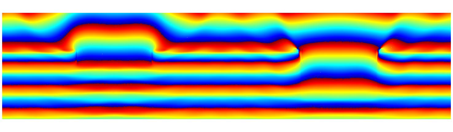
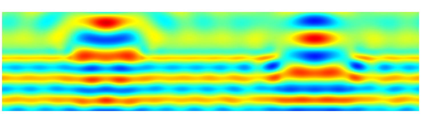
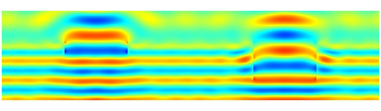
The effect of the phase shifting region is clearly visible, leading to 180 degrees phase difference of the light above the openings. Also the S and P components of the field show the phase difference:
In the project file, the FourierTransform post process is set, to obtain the transmitted diffraction orders of the mask:
PostProcess {
  FourierTransform {
    OutputFileName = "$THIS_results/ft.jcm"
    FieldBagPath = "$THIS_results/fieldbag.jcm"
    NormalDirection = Y
  }
}